Episodes

Tuesday Aug 11, 2020
Being Right Matters! When, Why and What to Simulate
Tuesday Aug 11, 2020
Tuesday Aug 11, 2020
Steve Sandler, electronics simulation and PI guru, prolific author, AEi Systems founder, and president of Picotest, joins the OnTrack Podcast for a “hold onto your seats” discussion of how he came to simulate the International Space Station for NASA, the intricacies of the James Webb Space Telescope, his flash of insight while improving WEBENCH®, modern board level issues, and his secret life as a pizza chef.
Steve will have a significant role in the virtual edition of AltiumLive coming up in October 2020. So get to know him, his new company Picotest, connect with him on LinkedIn, and even take a virtual tour of his lab!
Altium 365 Podcast Listener Discount
Show Highlights:
- The essential need for simulation: Steve Sandler and his upcoming role in AltiumLive 2020
- “...to be useful, it has to be fast”: key takeaways from the circuits simulation effort
- How the James Webb Space Telescope demonstrates the necessity of simulation
- Understanding why and what you’re simulating
- ”A whole new set of problems”: today’s board level issues
- Europa satellite; ground bounce in the printed circuit board
- Altium’s Ben Jordan’s go-to SPICE simulation book
- The ISS experiences a solar eclipse every 90 minutes: NASA, AEi Systems, and Steve’s most difficult simulation
- A brief history of the SPICE engine (Simulation Program with Integrated Circuit Emphasis)
- Brainstorm!—How Steve used a behavioral model to fix WEBENCH®
- Designers After Hours: from PI to (PI)zza; Steve’s secret life as a pizza chef
- ”I got bored…”: coming out of retirement to start Picotest
- Sandler on LinkedIn: take a virtual tour of Steve’s laboratory!
Links and Resources:
- Steve Sandler on LinkedIn
- Steve Sandler the Pi Guy. Watch his DIY Pizza.
- LOOK! Steve Sandler shared a video of his Home Lab.
- Picotest on LinkedIn
- Picotest website
- AltiumLive Registration Page
- Steve Sandler Amazon Author Page
Altium 365 Podcast Listener Discount
Tuesday Aug 04, 2020
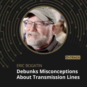
Eric Bogatin Debunks Common Misconceptions About Transmission Lines
Tuesday Aug 04, 2020
Tuesday Aug 04, 2020
Signal integrity expert, Dr. Eric Bogatin, has a new book whose mission is to establish a solid educational foundation in the essential principles of signal interaction with transmission lines. The multimedia eBook, Bogatin’s Practical Guide to Transmission Line Design and Characterization for Signal Integrity Application, is currently available from Artech House and can also be found on Amazon.
Dr. Bogatin is Signal Integrity Evangelist at Teledyne LeCroy, a leading provider of oscilloscopes, protocol analyzers, and test and measurement solutions. He joins the OnTrack Podcast to discuss his book and give us a sneak peak of his upcoming AltiumLive panel with Istvan Novak, Heidi Barnes of Keysight, and Steve Sandler of Picotest.
Altium 365 Podcast Listener Discount
Show Highlights:
- In addition to so much else, Eric Bogatin is a science fiction author! Check out his books Shadow Engineer, and S is for Space
- An overview of Eric’s new multimedia eBook, ‘Bogatin’s Practical Guide to Transmission Line Design and Characterization for Signal Integrity Application’
- ”I think the most confusing topic out there...is transmission lines”; how Eric’s book builds a solid foundation for anyone seeking clarification on transmission lines.
- Clarifying engineering’s most confusing issues
- Teledyne LeCroy’s new TDR calculator
- The practical nature of transmission lines: common misconceptions among engineers
- Embedded videos, demos, and calculations: how Eric’s multimedia book provides an interactive experience
- Hard copies, soft copies, ALL the copies: how and where to find Eric’s book(s)
- AltiumLive announcement
- The plain truth about split ground planes: Eric provides a sneak peak of his upcoming AltiumLive panel with Istvan Novak, Heidi Barnes of Keysight, and Steve Sandler of Picotest.
- ”There’s one case where you wanna use a split ground plane...”: Eric previews his upcoming demo on crosstalk reduction
Links and Resources:
Eric Bogatin on LinkedIn
Bogatin’s Practical Guide to Transmission Line Design and Characterization for Signal Integrity Applications
Artech House Publishers
Eric Bogatin Author Page on Amazon
Shadow Engineer (Fiction Scifi book by Eric Bogatin)
S is for Space (2nd Scifi book by Eric Bogatin)
Teledyne LeCroy Website
Signal Integrity Journal
Podcast Episode: Signal Integrity Evangelist Eric Bogatin, our Expert Insider to DesignCon 2020
Altium 365 Podcast Listener Discount
Wednesday Jul 29, 2020
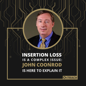
Insertion Loss is a Complex Issue: John Coonrod is Here to Explain It
Wednesday Jul 29, 2020
Wednesday Jul 29, 2020
Altium 365 Podcast Listener Discount
The OnTrack Podcast welcomes John Coonrod back to the show. John is Technical Marketing Manager at Rogers Corporation and a senior engineering professional with a rich background in PCB design, fabrication, processing, and modeling. John also has extensive experience with circuit materials, making him the ideal candidate for the topic of today’s podcast: insertion loss.
Show Highlights
- 01:45—Clarifying terms: a quick overview of Microstrips vs Striplines
- 02:20—Exploring laminates, multilayered circuits, and plated through-holes
- 06:42—Applying electromagnetic fields: a prerequisite for understanding insertion loss
- 09:25—The four components of insertion loss
- 13:10—RO4350B™; a friend to all fabricators?
- 15:10—Pros and Cons of electroless nickel immersion gold (ENIG)
- 18:13—John’s advice to design engineers on modeling for ENIG’s performance range
- 21:33—Navigating the relationship between solder masks and insertion loss
- 24:20—A call to viewers and listeners: Got a copper-related topic you’d like to hear John and Judy discuss? Submit your requests!
Resources:
John Coonrod on Linkedin
Rogers Corporation Website (Advanced Connectivity Solutions)
(Includes Coonrod’s corner videos, data sheets, calculators and more)
Autonomous driving Resource Page (Guides, Videos and Material selection)
ROG Mobile App (Resources accessible from your smartphone or tablet)
White Paper High Performance PCBs: Judy Warner, Chris Savalia, Michael Ingham
Altium 365 Podcast Listener Discount

Tuesday Jul 14, 2020
How To Actually Evolve During COVID-19
Tuesday Jul 14, 2020
Tuesday Jul 14, 2020
Angus Thomson is Senior Electronic Engineer and founder of CircuitBuilder, a brand new platform for simplifying the development of custom electronics out of Suffolk, England. Angus joins the OnTrack Podcast to share his experiences as CircuitBuilder’s founder, and to discuss the fine points of CircuitBuilder’s evolving business model, which has so far proven immune to the challenges of the global pandemic.
Altium 365 Podcast Listener Discount
Show Highlights
- Introduction to Angus Thomson
- ”I thought: there’s a better way to do this”—Angus’ road to entrepreneurship
- How CircuitBuilder utilizes Altium 365 to provide customers with realtime 3D views of their designs
- The CircuitBuilder growing network of engineers
- CircuitBuilder’s successful, lightweight recruitment process
- Proving it out in your own backyard: Angus on expanding market reach
- Transparency: How Altium 365 pushes CircuitBuilder beyond the errors of the past
- Design, Manufacture, or both? CircuitBuilder’s evolving business model
- The secret of CircuitBuilder’s resilience during the coronavirus health crisis
- Angus offers his insight on the future of design in a post COVID-19 world, and on CircuitBuilder’s role in that future
Resources:
Tuesday Jul 07, 2020
Tuesday Jul 07, 2020
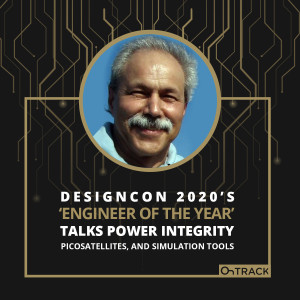
Istvan Novak, Principal Signal and Power Integrity Engineer for Samtec Inc. and winner of the DesignCon 2020 Engineer of the Year Award joins the OnTrack podcast to talk picosatellites, simulation tools, and the rising importance of power integrity.
Altium 365 Podcast Listener Discount
Show Highlights
- Introduction to Istvan Novak
- A brief look at Samtec Inc., the successful computer equipment manufacturing company headquartered in Indiana.
- Istvan’s path to becoming a Power Integrity expert
- CubeSats and the students who make them
- The challenges of dimensionality: has power integrity become more important than signal integrity?
- When Power Integrity is an afterthought
- The value of expert disagreement
- “Regardless of what we want to simulate, we can find good simulation tools to do it”: Good design and the challenges of modeling and simulation
- Closing thoughts; the first working Picosatellite; and the first electrosmog map of the globe
Resources:
- Istvan Novak on LinkedIn
- Samtec: gEEk spEEk SI Webinars.
- Samtec Silicon-to-Silcon Solutions Website
- The SI-List Archives
- Istvan Novak: DesignCon 2020 Engineer of the Year Award
- BUDAPEST UNIVERSITY OF TECHNOLOGY AND ECONOMICS Picosatellite
- Istvan Novak’s Electrical Integrity Website
- Picotest Website
- Signal Integrity Journal
- Design 007 Magazine, See pg. 38 Do You Really Need That Ferrite Bead in the PDN?
- First Electrosmog Map of the globe
Tuesday Jun 23, 2020
How Calumet Electronics Joined the Fight Against COVID-19 With Altium 365
Tuesday Jun 23, 2020
Tuesday Jun 23, 2020
The town of Calumet, with a population of barely seven-hundred, was once the booming epicenter of Michigan’s upper peninsula mining industry. When the industry began to fail, unemployment skyrocketed, and the townspeople sought local solutions for creating jobs that could sustain the town’s families.
Rob Cooke, Director of Engineering Services at Calumet Electronics Corp, joins the OnTrack podcast to discuss the Open Source Ventilator project, his experiences implementing Altium-365, and the radical decision business owners in that small town of Calumet, Michigan made more than 50 years ago, which led to the rise of Calumet Electronics Corp.
Altium 365 Podcast Listener Discount
Show Highlights
- Intro to Rob Cooke: how he got involved with Dugan Karnazes and the Open Source Ventilator Project.
- From copper ore to copper pours: Calumet, Michigan’s fascinating backstory.
- So what’s the hold-up? The right tool for avoiding excessive holds and other barriers to expedient design.
- Reality transcends the map: Altium-365 demos vs firsthand experience.
- The impact and implications of sudden hyper-efficiency at the designer, fabricator, and assembler level.
- The shock of realtime: “This is what can happen when things don’t go on hold!”
- Rob offers some final thoughts on the purchasing and quoting paradigm.
Resources:
- Rob Cooke on LinkedIn
- Calumet Website
- Open Source Ventilator Video
- AltiumLive 365 Demo
- Altium 365 product page
- Open Source Ventilator Project (OSV) Combats Ventilator Shortage
- Previous Episode with Rob Cooke: How to Conquer Data Package Problems

Tuesday Jun 16, 2020
How GreenSource Handles Microvia Reliability Issues With Jim Brown
Tuesday Jun 16, 2020
Tuesday Jun 16, 2020
Jim Brown of GreenSource Fabrication joins to discuss microvia reliability issues that so many people struggle with. GreenSource has been making great strides in this direction so listen now to learn how they’ve handled microvia reliability.
Altium 365 Podcast Listener Discount
Show Highlights
- Introduction to Jim Brown and GreenSource Fabrication
- A Brief History of GreenSource—becoming an open market supplier of PCBs in two phases
- ”Make it as automated as possible”—How GreenSource eliminates yield issues
- ”A well known issue”—exploring anomalies arising from stacked microvias
- Challenges presented by laser-drilling vias
- Virtual Meeting with ICP on July 15th and 16th
- Accelerated testing and the most reliable way of determining microvia reliability
- IST vs OM tester, which is preferred and what do they do
- Why GreenSource committed to OM testing
- Where to learn more about Jim Brown and GreenSource
- Outro and goodbyes
Resources:
- Jim Brown on LinkedIn
- Greensource Fabrication Website
- June OnTrack Newsletter
- The IPC Warning About Microvia Reliability for High Performance Products an article by Happy Holden
- IPC Microvia Reliability Summit Webinar on July 15-16, 2020
- Microvia Reliability in Ultra-High Density Interconnect Designs

Tuesday Jun 09, 2020
How to Transition Your Global Team to Altium 365
Tuesday Jun 09, 2020
Tuesday Jun 09, 2020
Jeremie Waller, Sr. Electrical Engineer at Quantel Laser, visits the OnTrack podcast to talk about infrared lasers, microplasma bursts, transitioning to Altium 365, and setting up user groups.
Work from Anywhere. Connect with Anyone.
Show Highlights
- An introduction to Jeremie Waller and Lumibird.
- Shock and awe: Class IV lasers and Lidar applications.
- A video demonstration: microplasmic bursts in the lab with the Merion C—a 100 millijoule 400Hz infrared laser.
- ”Going to the cloud just sounded like the right thing to do.” How Jeremie and his team became Altium 365 beta users at the outset of the pandemic.
- eedback on the transition to Altium 365 from Firmware Engineers, Material Managers, and
- Fabricators.
- Learn, connect, and get inspired: Adopting Altium and the importance of review meetings and training.
- Lost in Translation: working in a global work environment.
- Adventures in setting up Altium Live user groups.It takes less time than you think. Run by you, the users; and run your way.
Resources:
Quantel Lasers by Lumibird website
Introduction to Lumibird (Video)
Jeremie Waller LinkedIn profile
To Learn more about starting an Altium User Group:
Wednesday Jun 03, 2020
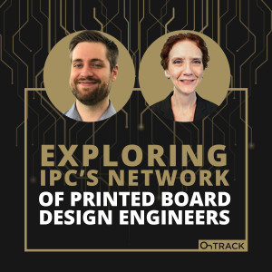
Exploring IPC’s Network of Printed Board Design Engineers
Wednesday Jun 03, 2020
Wednesday Jun 03, 2020
The renowned global trade association known as IPC has put together a network of printed board design engineering affiliates under the name IPC Design. IPC Design’s affiliates are comprised of PCB design engineers across the globe who are working to advance the art and science of printed design engineering.
IPC Design’s Patrick Crawford and Teresa Rowe join the OnTrack Podcast
Work from Anywhere. Connect with Anyone.
Show Highlights
- What is IPC Design, and what is its primary mission?
- Increased global presence and participation: How IPC is molding its future.
- IPC Design’s worldwide buy-in, its fresh new participants, and how the quarantine has affected participation.
- Has productivity gone up since quarantine?
- Lessons in remote working and the importance of taking time for yourself.
- Between January 2020 and now.
- What’s in store for the future: IPC’s collaborative content model.
- America, Europe, and Asia: IPC’s leadership group and global design committee.
- IPC Design is looking to fill a leadership role in Asia.
- What’s in it for you, the designer? Teresa and Patrick count the ways designers will benefit from IPC Design.
- ”Let’s start up a chapter!”: How individuals, student groups, and companies can get affiliated with IPC Design.
- Translators of the world, connect! How IPC Design can serve and collaborate with STEM groups all over the globe.
Resources:
Teresa Rowe on LinkedIn
Patrick Crawford on LinkedIn
IPC Website
Link to IPC Design webpage
Link to IPC Design enrollment page
Patrick Crawford’s video presentation on IPC Design
Realtime with IPC
IPC CEO John Mitchell on the Impact of COVID-19 on the Electronics Supply Chain
Work from Anywhere. Connect with Anyone.

Tuesday May 26, 2020
Best Practices Cultivating a Healthy and Productive Remote Working Environment
Tuesday May 26, 2020
Tuesday May 26, 2020
A leading research and advisory company, Gartner, Inc., found that nearly 75% of the 317 CFOs and business finance leaders they surveyed planned to move at least 5% of their formerly on-site workforce into permanently remote positions even after the COVID-19-related quarantines have ended.
Zach Peterson, prolific technology content writer, scientist/engineer, and owner and CEO of Northwest Engineering Solutions, joins the OnTrack Podcast to examine the implications of this finding, and to share best practices for creating a viable and productive remote working environment from both a manager’s and employee’s perspective.
Work from Anywhere. Connect with Anyone.
Show Highlights
- The business case for remote teams, and a worldwide freelancing network’s shocking statistic about the future of remote work
- Suggestions for managers and employees that will ensure their remote teams remain viable and productive
- The importance of setting clear expectations for your remote team
- Why you shouldn’t “babysit” your remote workers; the importance of allowing workers to work within their comfort zones
- Setting clear boundaries: how remote working can upset our work/life balance, and what steps one should take to cultivate it
- Tackling the myth of slackers in the remote work environment
- Ideal tools for the remote working environment
- “Engage earlier rather than later”—tips for maintaining the relationship between design engineers and manufacturers in a remote environment
Resources:
Zach’s Technical Articles on Altium.Com
How to Manage a Remote Team for Electronics Design
Signal Integrity Article Coronavirus Shows how Quickly Electronics Supply Chains Can

Tuesday May 19, 2020
Innovators Around the Globe Contribute to Coronavirus Intervention
Tuesday May 19, 2020
Tuesday May 19, 2020
Work from Anywhere. Connect with Anyone.
Colin Keogh PhD, CEO & Founder at The Rapid Foundation, has been on the front lines of the effort to combat ventilator shortages ever since a Facebook group called Open Source COVID-19 Medical Supplies (OSCMS) first presented the problem.
As cofounder of Open Source Ventilator (OSV) Ireland and a member of its core team, Colin offers his uniquely qualified perspective on open source innovation: its obstacles, its advantages, and its impact on world governments and regulatory bodies both now and in the future.
Show Highlights:
- Racing a pandemic: How Open Source Ventilator (OSV) Ireland turned a single Facebook post into an enterprise-scale organization composed of hundreds of engineers around the world.
- Silver linings in the time of COVID-19: evaluating the role of innovators in an epidemic, and how the lines separating government bodies and open source innovators become blurred in times of need.
- What young engineers are bringing to the table, and how the contributions of open-source innovators compare to that of Fortune 100 companies of today.
- ‘Fail fast and break things’ vs. the traditional approach to engineering: reconciling the two faces of modern innovation.
- Slack, Zoom, and Altium: the collaborative tools OSV Ireland used to produce solutions quickly while managing its unprecedented explosive growth.
- Welcome aboard; solutions are required: How OSV turned the usual medical design process on its head.
- ‘The provision of information is gonna be very important’: How the pandemic has affected the navigation of medical device regulation from country to country, and what innovators can expect from regulatory bodies in the future.
- How new revelations brought about by the pandemic will affect the interaction of medical device developers and regulatory bodies in the future.
- Colin’s delivers his unique perspective of the overall impact of COVID-19 on the world, and how engineers will use this experience to continue to overcome the obstacles ahead.
Links and Resources:
Colin Keogh on LinkedIn
Open Source Ventilator Website
OSV on Twitter
OSV on Linkedin
Fundraiser by Dugan Karnazes : Open Source Ventilator
Watch: Engineering Together to Save Lives
Sunday May 10, 2020
Leigh Gawne on the Launch and Significance of Altium 365
Sunday May 10, 2020
Sunday May 10, 2020
Work from Anywhere. Connect with Anyone.
Altium 365 is here, and its CAD-aware approach to cloud-based design is already cutting lead times down by orders of magnitude. How will this affect designers, and how will it affect the electronics industry as a whole? Leigh Gawne, Chief Software Architect at Altium 365, answers these questions and more. Get an exclusive look inside the impact Altium 365 is having on the electronics industry and learn more about this powerful new tool.
Show Highlights:
- Up until this point, ECAD has been confined to the desktop. Leigh explains how Altium 365 breaks this trend, allowing anyone with an internet-enabled device to interact and collaborate in the design process—directly from a web browser.
- No download necessary: Altium 365 ditches the software download for manufacturers and other stakeholders.
- Is the Google Drive comparison accurate? Leigh demonstrates how Altium 365’s approach to ‘CAD-awareness’ pushes its capabilities far beyond the reach of ordinary cloud-based design tools.
- Is this design manufacturable? Resolving essential questions with the click of a button in Altium 365, allowing designers to instantly share designs as a live view or as a snapshot.
- Never lose a comment thread again. Leigh explains how Altium 365’s ‘contextual commenting’ feature allows designers to attach comment threads right to relevant features in the design.
- Customers, procurement personnel, and project management: How Altium 365 facilitates seamless interaction with secondary stakeholders.
- Altium 365’s option for browser-driven design review minimizes mistakes and pulls more stakeholders into the chain.
- Supply chains are dynamic and are often subject to radical, unexpected changes, especially in a pandemic. Leigh breaks down Altium 365’s “baked-in” Octopart capability, which allows designers to monitor their supply chains in real-time.
- Navigating the ‘new normal’: Leigh examines Altium 365’s important and powerful role for product design in the post-coronavirus age.
- Out the door in 30 days: Reviewing Altium 365’s integral role in the Open Source Ventilator Project’s incredible success story.
- Success all around: How Altium 365 makes it trivial to duplicate another company’s achievements.
- Leigh looks at the future of the electronics in the wake of this powerful new tool.
Links and Resources:
Exclusive Sharable Listener Discount Link
Altium Designer-Altium 365
Altium 365 Customer Stories Videos: Skyship, Arduino, Project March
Altium 365 Webpage
Altium 365 LIVE Demo from AltiumLive 2019 with Leigh Gawne
Open Source Ventilator Podcast with Dugan Karnazes
Now you can get the ultimate PCB design productivity with the easiest platform for PCB design. Easily communicate design changes to your team with Altium 365.
Tuesday May 05, 2020
Altium 365: Work from Anywhere, Connect with Anyone
Tuesday May 05, 2020
Tuesday May 05, 2020
Altium 365 has launched in the midst of a worldwide quarantine effort—a time when companies have drastically reduced the in-office workforce, and financial constraints and travel restrictions have never been tighter.
Altium’s VP of marketing, Lawrence Romine, joins the OnTrack Podcast to explain how Altium 365 removes the obstacles presented by the lockdown effort, why it’s the perfect tool for the post-coronavirus environment, and how the launch timing couldn’t be more serendipitous.
Work from Anywhere. Connect with Anyone.
Show Highlights:
- Altium 365 has launched on schedule; a brief look at why the timing couldn’t be more perfect.
- Working remotely. The Altium 365 cloud based platform which Altium Designer and Concord Pro run on.
- Seamless integration: the symbiotic relationship between Altium Designer and Altium 365.
- Arduino, SkyShips, and you: the various types of Altium 365 users, and how the addition of new features addresses their individual needs.
- Flattening the curve: Altium’s conscientious approach to the learning curve when adding new features.
- Design Reviews in a pandemic—a use case: How Altium 365 removes the obstacles presented by a remote work environment.
- Some users describe the experience of Altium 365’s cloud-based real-time collaboration as “similar to working in Google Docs”. Lawrence elaborates.
- It’s as easy as sending a link: How Altium 365 frees up budgets by eliminating excessive travel, phone calls, and emails.
- “Simplicity is the ultimate expression of sophistication”: Lawrence recalls an automotive experience from his life in praise of Altium 365’s design ethic.
- As simple as using a web browser: How sales personnel are utilizing Altium 365 as a demonstration tool for prospective clients.
- Lawrence’s predictions about the farside of the COVID-19 calamity.
Links and Resources:
Exclusive Sharable Listener Discount Link
Altium Designer-Altium 365
Altium 365 Customer Stories Videos: Skyship, Arduino, Project March
Altium 365 Webpage
AltiumLive: Altium 365
Altium 365 Security
Now you can get the ultimate PCB design productivity with the easiest platform for PCB design. Easily communicate design changes to your team with Altium 365.
Work from Anywhere. Connect with Anyone.
Tuesday Apr 28, 2020
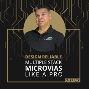
Design Reliable Multiple Stack Microvias Like a Pro
Tuesday Apr 28, 2020
Tuesday Apr 28, 2020
Gerry Partida is a 36 year veteran of the PCB industry, and spent twenty of those years working in boardshops. He is currently a Senior Field Application Engineer for Summit Interconnect, where he and his colleagues have made a fascinating discovery about the reliability of multiple stacked microvias. Gerry and his team are still collecting data on this finding, but he joined us on OnTrack to share a firsthand account of what he knows!
Work from Anywhere. Connect with Anyone.
Show Highlights:
- Gerry shares his industry background and introduces Summit Interconnect, the second largest printed circuit board manufacturer in North America.
- What is a microvia? A manufacturer’s perspective.
- The first step is recognizing there’s a problem: a brief overview of the issue with multiple (more than two) stacked microvias.
- To boldly go where no one has gone before: In the absence of an IPC standard, Gerry shares the recommended distance between stacked microvia and mechanically drilled holes.
- Gerry’s advice on how to avoid overloading your designs.
- Gerry discusses IPC-6012E and the need for performance testing in the absence of adequate scopes (over 500x).
- OM testers: What are they, how prevalent are they, and how can they add value to your company?
- OM testing: Reflow simulation and thermal shock testing—its value and its scope.
Links and Resources:
Gerry Partida on LinkedIn
Summit Interconnect
IPC-6012E
Now you can get the ultimate PCB design productivity with the easiest platform for PCB design. Easily communicate design changes to your team with Altium 365.
Monday Apr 20, 2020
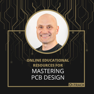
Online Educational Resources for Mastering PCB Design
Monday Apr 20, 2020
Monday Apr 20, 2020
Ben Jordan drops in to share details on Altium’s central hub for online education resources: hands-on video, feature documentation, and tips and tricks for navigating and mastering Altium’s software. Ben is a Computer Systems and PCB Engineer with more than 20 years of embedded systems, FPGA and PCB design. See why we’re now calling him “the Dean of Altium Academy”. Here’s another podcast you can’t afford to miss!
Try Altium Designer 20 + Altium 365 Today
Show Highlights:
- Altium’s free webinar series: Why Altium is doubling down on webinars, where to find them, and how to use them to your advantage.
- Zig Ziglar and the secret of success.
- The Altium Academy YouTube channel: hands-on video, feature documentation, and tips and tricks for navigating Altium’s software.
- On providing an easy-to-find central information resource hub on the Altium domain—where your questions about all Altium products can be answered in detail.
- How the complexity of CAD software speaks to the nature of engineering work
- Ben offers users some insider info—a reason Altium users should check out Altium Academy’s YouTube Channel right now.
- Who is in charge of the public health? Ben offers an eye-opening perspective on the role of engineers in society.
- Ben discusses new challenges being faced during the Covid-19 epidemic.
- Judy revisits how Dugan Karnazes was able to coordinate a worldwide engineering team’s spin-up of an early Open Source Ventilator design within 24-hours.
- Ben describes his visit to General Atomics’ tokamak.
- The importance of staying connected: Ben and Judy offer closing statements and advice for all of us as we weather the Covid-19 crisis.
Links and Resources:
Ben Jordan on Linkedin
Altium Academy Virtual Sessions
jedec.org
Tuesday Apr 14, 2020
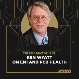
The EMC Doctor is in: Ken Wyatt on EMI and PCB Health
Tuesday Apr 14, 2020
Tuesday Apr 14, 2020
The OnTrack Podcast is pleased to welcome Ken Wyatt (also known as the ‘EMC Doctor’). Ken began his career as a designer in the aerospace industry, and later worked for Hewlett Packard, where he found that his background in RF and Microwave engineering helped prepare him for his role as an Electromagnetic Compatibility (EMC) Engineer. His work has since taken him all over the world, where he develops and provides in-house training and delivers presentations and live demonstration; definitely unique among presenters!
Retiring early in 2008, Ken has since become a prolific author, co-authoring three books, including his latest, in which he identifies why products fail to meet EMI/EMC regulatory standards: ‘EMI Troubleshooting Cookbook for Product Designers’.
Ken currently provides seminars on a variety of EMC related topics—touching on subjects not often taught at the university level. He also provides EMC consultation, EMC compliance and precompliance testing, design reviews, and training services for commercial, military/aerospace, scientific, consumer, and computing industry sectors.
See What's New in Altium Designer
Show Highlights
- Ken lays out his career path, from his beginnings in the aerospace industry, to his current role as a consultant.
- ‘EMI Troubleshooting Cookbook for Product Designers’—a quick look at the book Ken co-authored with Patrick G. André.
- Addressing the prevailing trends in stackups and board design in general.
- Old habits die hard: Why the PCB is the heart of most EMI and EMC issues today, and pitfalls to avoid to move past these issues.
- Signals as the flow of electrons in copper traces and wires: How our education may have left out the whole story with respect to high frequency design.
- How simultaneous trends toward diminishing device size and the Internet of Things contributes to desensing and other issues on PCBs.
- Staying “in the know”: Keeping up with our evolving understanding of the physics of PC boards and signal propagation is always challenging. Ken lays out some ways designers can stay up to speed.
- Why Electromagnetic Compability programs at the university level are few and far between, and how Missouri University of Science and Technology stands out among them.
- Case Studies: The trouble with dog trackers and blood transfusion machines. Ken discusses some challenges he’s come across in the field.
Resources:
Short video on the book with co-author Patrick André
Ken Wyatt on Twitter: @emc_guru
See What's New in Altium Designer

Tuesday Apr 07, 2020
Open Source Ventilator Project (OSV) Combats Ventilator Shortage
Tuesday Apr 07, 2020
Tuesday Apr 07, 2020
The Novel Coronavirus (SARS-CoV-2) epidemic appears to be slowing in countries practicing social distancing measures, but we’re not out of the water yet. Serious medical equipment shortages continue to dog hospitals around the world, and officials are bracing for worst-case scenarios: medical triage.
Here’s how one entrepreneur channeled his concern for a high-risk family member into action, using his training and resources to aid the fight against equipment shortages. Dugan Karnazes, founder and CEO of Velocity Research, joined the Open Source Ventilator project (OSV), a world-wide effort to develop and design a simple, low-cost emergency-use ventilator to aid in the treatment of COVID-19 patients.
Karnazes joined Judy Warner on the OnTrack Podcast to discuss these efforts, and detailed how he and the OSV project were able to enlist the help of hundreds of engineers and medical professionals, as well as support from corporations like Ford, Worthington, CircuitHub, DigiKey, and Altium.
Show Highlights
- Dugan Karnazes discusses his background in Physics and Electrical Engineering and his career in R&D.
- A small team with a broad skill set: Dugan on starting Velocity Research, and the value building teams with diverse technical backgrounds.
- Dugan shares a personal account of how the threat of COVID-19 affects him, and how he turned heartbreak into motivation to join the front-lines in the fight against equipment shortages during the COVID-19 crisis.
- Open Source Ventilator project (OSV) and how it is addressing the worldwide ventilator shortage.
- How the Open Source Ventilator project (OSV) became a massive collective of worldwide contributors.
- Casting a wide net: How Dugan helped to draw in more than 800 engineers worldwide to offer their skills to the OSV project.
- Altium responds to the OSV project’s call.
- The Open Source Ventilator project turns to Altium 365: How Dugan leveraged Altium’s software to add hundreds of engineers to the Open Source Ventilator project, and went from having a need to having a distributed solution within 24 hours.
- Dugan explains how collaboration (and a bit of synchronicity) between Altium, Circuithub, Digi-Key, and Worthington helped reduce critical OSV development cycles from weeks to mere hours.
- Enter the medical professionals: Dugan’s contact at Spectrum Health Innovations sets up a team of pulmonary specialists, respiratory therapists, and other medical industry professionals to provide live feedback on OSV project developments.
- Ford Motor Company joins the fight—shares resources with the OSV project and commits to making 50,000 ventilators: How the automotive giant is leveraging existing hardware and supply chains to help the OSV project while developing their own ventilators.
- Dugan discloses the sobering prediction that Michigan was 5-10 days away from hitting capacity on ventilators, and details the horrifying medical triage decisions this would entail for medical professionals.
- Dugan shares diagrams and photographs of the OSV project’s ventilator prototype!
Fundraiser by Dugan Karnazes : Open Source Ventilator
Resources:
Look, the ventilator is coming together! Dugan shares 3D rendering and an actual photo.
Tuesday Mar 31, 2020
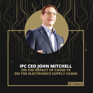
IPC CEO John Mitchell on the Impact of COVID-19 on the Electronics Supply Chain
Tuesday Mar 31, 2020
Tuesday Mar 31, 2020
A $2 trillion coronavirus relief bill was signed into law on Wednesday, March 25th. The bill will, among other things, send money directly to American citizens, small businesses, and troubled corporations, all of which have been greatly affected by COVID-19 and the resulting lockdowns.
In this podcast, Dr. John Mitchell, president and CEO of the IPC trade association, discusses the effects of the SARS-CoV-2 crisis on the electronics industry, enumerates the IPC’s efforts at mitigating those effects around the world, and elaborates on IPC’s Roadmap to Economic Recovery.
The IPC has been helping the electronics industry navigate dramatic changes since 1957. Here, Dr. Mitchell demonstrates why the current coronavirus pandemic is no different.
Show Highlights
- Dr. John Mitchell provides a brief description of the trade association known as IPC, and elaborates on its role in ensuring the collective success of the electronics industry as a whole, both in the past and during the current COVID-19 crisis.
- IPC’s relationships with world governments, and its advocacy efforts since the advent of the COVID-19 epidemic.
- John delivers some encouraging news out of China.
- Manufacturers have stepped up to address the pressing need for ventilators and masks: how IPC works with government to direct those efforts.
- Coronavirus, the $2 trillion stimulus package, and IPC’s Roadmap to Economic Recovery.
- Have manufacturing jobs returned to the U.S.? How recent U.S. tariff restrictions have affected the electronics industry and the world.
- Your work is essential: Shelter-in-Place orders and IPC’s response.
- A quick rundown of IPC’s ‘COVID-19 (Coronavirus): Economic Impact on Electronics Manufacturing Industry Webinar’.
- Online ‘Live Training’ and the advent of virtual-proctoring: John reveals how COVID-19 is affecting IPC’s online education and training, and what the organization has done to adapt.
- How the shutdown has hastened progression toward industry standards.
Resources:
IPC Coronavirus Updates - New info added daily
IPC Online Learning in PCB Design
IPC Global Advocacy Update Reports
See What's New in Altium Designer
Tuesday Mar 24, 2020
Connectors for High-Speed Applications with Jason Ellison
Tuesday Mar 24, 2020
Tuesday Mar 24, 2020
Jason Ellison is a Signal Integrity Engineer and graduated from Penn State University with a Master’s of Science in Electrical Engineering. He currently develops high-speed interconnects, and calibration and automation technology for Amphenol out of Dillsburg, Pennsylvania. Jason has also written a number of articles for Altium’s PCB Design Blog and is a DesignCon technical program committee member, as well as an active IEEE member.
Show Highlights
- Form, Fit and Function: Jason expands on the demands driving connector technology relative to high speed.
- With regard to signal integrity, connectors have their own issues—reflection, insertion loss etc. Jason reviews the challenges these constraints introduce at the board level, and tells us how to deal with them.
- Why you should let the PCB houses tell you what you need to do to make your board work, instead of vice versa.
- The importance of knowing what your PCB houses are capable of.
- Recurring issues in Signal Integrity and how to mitigate them.
- Jason shares details of his secret weapon for generating consistently correct results for differential impedance calculations.
- As chips become more dense, it’s becoming increasingly difficult to manage crosstalk—and lowering density is not an option! But there’s hope… Jason drops some advice on how to get the greatest amount of added signal at the lowest cost.
- Designers After Hours: Jason surprises us by recalling the precise moment he decided to become an electrical engineer, and tells us a little bit about his hilarious hobby.
Resources:
Jason Tricks of the Trade Article
PCB Handbook
Jason Ellison’s Blogs
Jason Ellison on LinkedIn
See What's New in Altium Designer
Wednesday Mar 18, 2020
COVID-19 Electronics Global Industry Update with Mike Buetow
Wednesday Mar 18, 2020
Wednesday Mar 18, 2020
COVID-19 has impacted daily life and supply chains. Here we bring to you the latest information to help you prepare the best possible response during this unprecedented time. As an electronics industry veteran, Mike Buetow, Vice President and Editor in Chief at PCD&F Circuits Assembly, is uniquely qualified to provide context on the COVID-19 crisis─because he also studied epidemiology. Learn how the electronics industry and supply chains are responding to the coronavirus quarantine, and how this will affect the electronics industry at large in this global industry update.
Click here to watch the video.
Show Highlights
- An Electronics Industry ‘State of the Union’: Mike analyzes emerging trends over the last four weeks, and offers his best forecast for how the industry will be affected by COVID-19.
- A quick breakdown of coronavirus mitigation techniques major companies are using.
- Trade Associations (e.g., IPC, SMTA, TCPA, IEEE) and their strategies for buffering against the effects of COVID-19.
- The impact of the COVID-19 travel restrictions and shut-downs on designers and OEMs.
- When some work can’t be done remotely: CDC recommendations against gatherings, and how EMS companies and fabricators are handling it.
- Mike responds to questions and comments from industry insiders.
- How will the coronavirus impact the industry’s dependence on China?
- Have we gotten better at weathering supply shortages? Comparative responses to electronics shortages and what we can expect from ripples in the supply chain due to COVID-19.
- ”You can’t close your borders to a disease...” Mike speaks from his background as a former student of epidemiology.
- Stress test! How 2020 will prove or disprove the effectiveness of the EMS industry’s supply chain.
- Will the COVID-19 quarantine amplify trends toward telecommuting?
Links and Resources
Twitter @mikeBuetow
Mike Buetow on Linkedin
Printed Circuit Design and Fab
Circuits Assembly website
OnTrack Podcast: Mike Buetow on PCB West

